Attached files
| file | filename |
|---|---|
| 8-K - 8-K - Versum Materials, Inc. | form8-k12112018.htm |

VERSUM MATERIALS TECHNOLOGY INTRODUCTION

2 FORWARD-LOOKING INFORMATION This presentation contains, and management may make, certain “forward-looking statements” within the meaning of the safe harbor provisions of the U.S. Private Securities Litigation Reform Act of 1995. Forward-looking statements may be identified by references to future periods, and include statements about our anticipated growth, profitability and margins; our investments in new markets, new products, capacity and productivity; our ability to compete successfully as a leading materials supplier to the semiconductor industry and obtain next generation node opportunities; industry outlook; anticipated customer demand; and other matters. The words “believe,” “expect,” “anticipate,” “estimate,” “continue,” “could,” “intend,” “may,” “plan,” “potential,” “predict,” “seek,” “should,” “forecast,” “guidance,” “outlook,” “opportunity,” “growing” and similar expressions, among others, generally identify forward-looking statements, which are based on management’s reasonable expectations and assumptions as of the date the statements were made. These statements involve a number of risks, uncertainties and other factors that could cause actual results to differ materially, including without limitation the following: product supply versus demand imbalances in the semiconductor industry or in certain geographic markets may decrease the demand for our goods and services; our concentrated customer base; the dependence of our DS&S segment upon the capital expenditure cycles of our customers; our ability to continue technological innovation and successfully introduce new products to meet the evolving needs of our customers; our ability to protect and enforce our intellectual property rights and to avoid violating any third party intellectual property or technology rights; unexpected interruption of or shortages in our raw material supply; inability of sole source, limited source or qualified suppliers to deliver to us in a timely manner or at all; hazards associated with specialty chemical manufacturing, such as fires, explosions and accidents, could disrupt operations; increased competition and new product development by our competitors, changing customer needs and price increases in materials and components; operational, political and legal risks of our international operations; increased costs due to trade wars and the implementation of tariffs; the impact of changes in environmental and health and safety regulations, anticorruption enforcement, sanctions, import/export controls, tax and other legislation and regulations in the U.S. and other jurisdictions in which Versum Materials and its affiliates operate; our available cash and access to additional capital may be limited by substantial leverage and debt service obligations; possible liability for contamination, personal injury or third party impacts if hazardous materials are released into the environment; cyber security threats may compromise our data or disrupt our information technology applications or services; fluctuation of currency exchange rates; costs and outcomes of litigation or regulatory investigations; the timing, impact, and other uncertainties of future acquisitions or divestitures; and other risks, uncertainties and factors discussed in the company’s Form 10-Qs, Form 10-K and in the company’s other filings with the U.S. Securities and Exchange Commission available at www.sec.gov or in materials incorporated therein by reference. The company assumes no obligation to update or revise any forward-looking statements.

VERSUM HELPS ADVANCE A WORLD DRIVEN BY EVER-GROWING INTERCONNECTIVITY Data Centers Servers Big Data Smartphones Healthcare MPUs PC/Tablets ASICs Security MCUs Storage Class Memory Smart Homes Analog Networks Smart Cities DRAM Wearables Robotics NAND Automotive VNAND Social Media Displays Industrial Infotainment LEDs Gaming Transportation MEMs Virtual Reality Mobile Computing Artificial Intelligence 3

VERSUM MATERIALS DIVERSIFIED PORTFOLIO FOCUSED ON TECHNOLOGY DRIVEN SEMICONDUCTORS SEGMENTS FOCUS AREAS KEY PRODUCTS • Advanced Materials • Advanced Deposition Materials for Thin Films • CMP Slurries and Post CMP Cleans MATERIALS • Formulated Products for Surface Prep & Clean • Process Materials • Deposition • Clean & Etch • Dopants

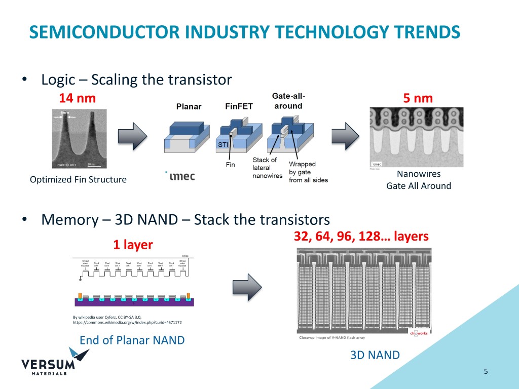
SEMICONDUCTOR INDUSTRY TECHNOLOGY TRENDS • Logic – Scaling the transistor 14 nm 5 nm Nanowires Optimized Fin Structure Gate All Around • Memory – 3D NAND – Stack the transistors 32, 64, 96, 128… layers 1 layer By wikipedia user Cyferz, CC BY-SA 3.0, https://commons.wikimedia.org/w/index.php?curid=4571172 End of Planar NAND 3D NAND 5

6

7 GLOBAL R&D LOCATIONS Technical Depth and Customer Responsiveness Tempe, AZ Planarization, SP&C ADM Organosilanes Carlsbad, CA ADM Organosilanes Banwol Tempe Hometown Pyeongtaek Hometown, PA Chupei Scale Up Engineering , Process Carlsbad Chudong Materials, ADM Organometallics Chupei, TW Surface Preparation & Cleaning Chudong, TW Planarization Banwol, KR Advanced Deposition Materials Pyeongtaek, KR Planarization 7

TECHNOLOGY ORGANIZATION KEY SKILLS 3 Business Technology Managers Materials Technology – Advanced Deposition Materials – Computational Modeling – Process / Scale Up Engineering – Planarization – Material Characterization – Surface Preparation & Cleaning – Interfacial Engineering Chemistry 2 Technical Capabilities Managers – Silicon Chemistry – Process / Scale Up Engineering – Organometallic Chemistry – Advanced Analytical – Organic Formulations Chemistry – Fluorine Chemistry Semiconductor Processing – Thin Film Deposition – Wafer Cleaning – Wafer Polishing – Process Integration Advanced Analytical – Gas and Wet Chemical Chromatography – Particle size and distribution – Mass Spectrometry – Metals Analysis 8

ADVANCED DEPOSITION MATERIALS Atomic Layer Deposition Organosilanes • Dielectric Films 3 Dimensional Devices • Patterning Films • Etch Stop Layers Flowable Films – Gap Fill Organometallics • Conductors • Barrier Films • Capping Layers ADM Precursor Synthesis & Scale Up ADM Applications Capability 9

PLANARIZATION TECHNOLOGY Chemical Mechanical Planarization CMP Slurries – Post CMP Cleans PLA Formulation Capability PLA Applications Capabilities 300 mm 300 mm Metrology 10

SURFACE PREPARATION & CLEANING Post Etch Residue Residue Free Features Multi-component formulations • Solvents • Etchants • Inhibitors . . • Oxidizers .. . . • Buffers . SP&C Chemical Formulation Capability SP&C Applications Capability

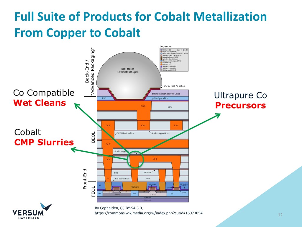
Full Suite of Products for Cobalt Metallization From Copper to Cobalt Co Compatible Ultrapure Co Wet Cleans Precursors Cobalt CMP Slurries By Cepheiden, CC BY-SA 3.0, https://commons.wikimedia.org/w/index.php?curid=16073654 12

TEMPE TECHNOLOGY FACILITY Tempe Research & 300 mm Integration Center Planarization Applications PM Applications 300 mm CMP Tools 300mm Etch Tool SP&C Formulation Lab & Pilot Plant ADM Applications 300 mm Deposition Tools 13

THANK YOU QUESTIONS 14
